Variable SMPS LED Supply
Concept
A switched mode current supply, adjustable via a logic-level PWM signal to realize a dimmable LED. This can be integrated into various projects, including an adjustable reading light or a sunrise alarm clock.
Essential Components
- LT3474
- Step-down LED driver, up to 14 V @ 1 A output. The LT3474-1 variant without open circuit protection can go to higher voltages, but
- Switching frequency and maximum output current are adjustable.
- Dimmable using PWM, 400:1 range with a minimum pulse width of 40 μs.
- Requires an external inductor and diode, and optionally an additional transistor for optimal PWM behavior. May require more than 14 V, however, depending on color and drive current.
- LedEngin LZ1 Series
- Single-die emitter structure, 1 A absolute maximum current, with very bright output.
- LZ4 series 4-die emitters are the next step up, but dissipate more heat and will require current derating.
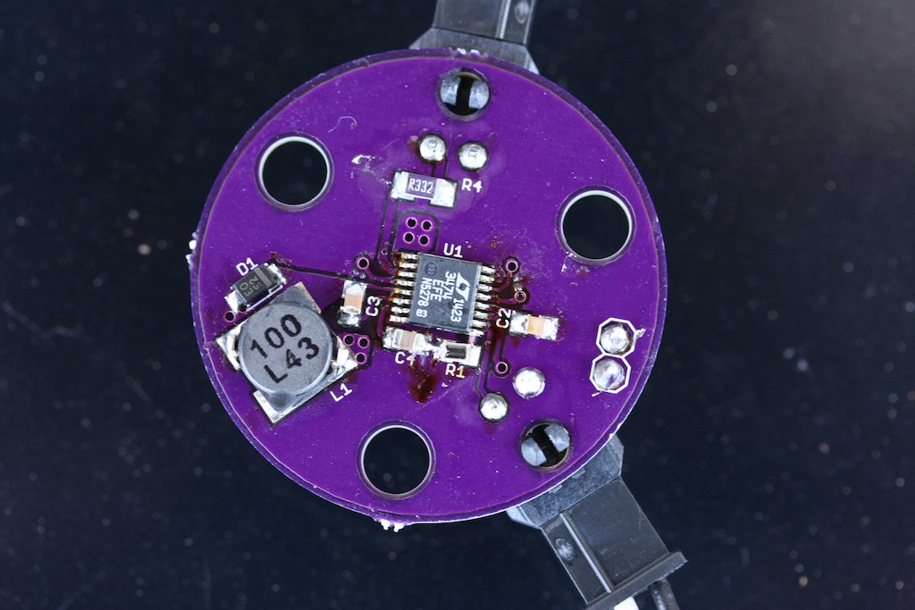
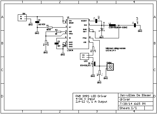
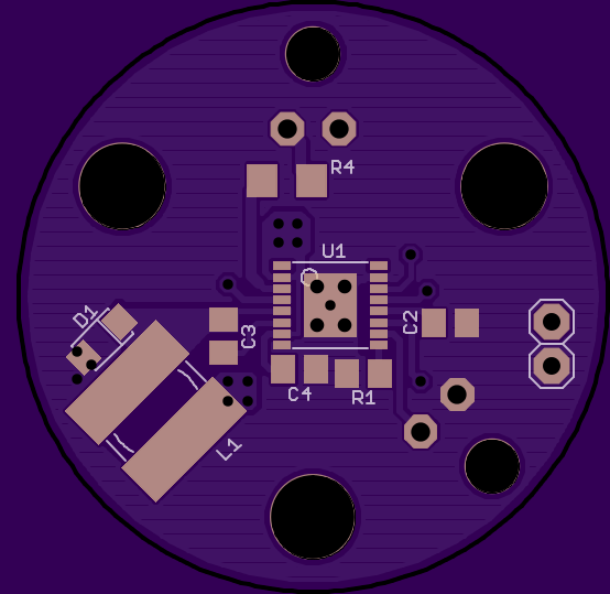
Schematic and Board
The schematic is very straightforward, based on the example application in the LT3474 datasheet.
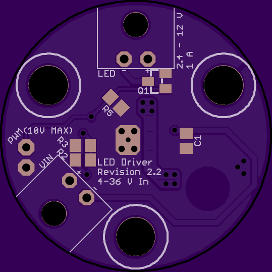
Multiple revisions have been created, to try out various layouts, connectors and such. Revision 2 of the board was made to fit behind an Ohmite SA-LED-113E heatsink
Observations
- The board warms up noticeably. A good ground plane as heatsink and a good connection between the exposed pad and the board is essential.
- The PWM pin is logic level input only. Forcing the LT3474 on by connecting it to Vcc for input voltages > 5 V will lead to arcing between PWM and GND pins, and the eventual destruction of the device.
- Molex Pico-EZMate™ connectors are compact and flush, but too fiddly to hand-assemble. Micro-Fit 3.0™ connectors work very well.
- PWM control works as expected. It will be necessary to reduce the output current, however, because even at 700 mA the LED is blindingly bright.
Issues
- Revision 2.1
- Not enough space around mounting holes for #10 screw heads and spacers
- Revision 2.2 (tested on 2014/08/09)
- Layout
- ”+” and “-” signs on the VIN connector are reversed.
- C4 is a bit too close to U1 to easily handle with tweezers. R2 and R3 may also be too close.
- Pads of D1 could be a little longer, and of Q1 a little narrower.
- Problems: A test board with R3 left out produces very low (<100 mA) output current for reasons so far unknown. Another is shorted on a number of pins, possibly a production fault.
- Layout