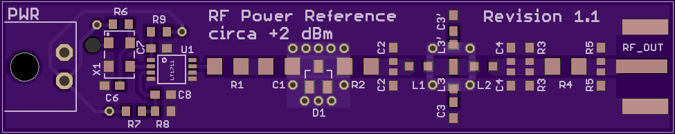
RF Power Reference
Introduction
This design is based off of W1GHz’s small project design, also published in QST April 2007. It feeds the output of a crystal or MEMS oscillator into a diode clipper to generate a square wave with a fixed voltage and then filters out the harmonics to reduce this to a sine wave. The filter is matched to 50 Ω (W1GHz uses a Chebyshev filter), but an additional output attenuator helps improve the matching.
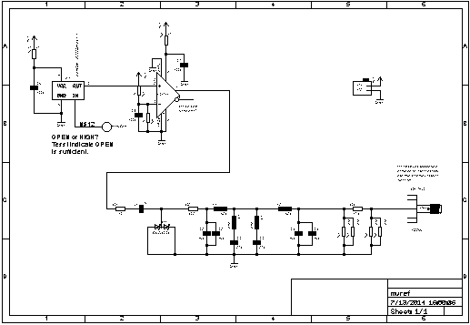
I redesigned the board for SMD components and using 50 Ω coplanar waveguide. In addition, the output impedance of the oscillator I intended to use was around 10 kΩ, so I added a comparator as a buffer. The schematic and board design were done in Cadsoft EAGLE, and the board and stencil is currently being prototyped by OSH Park and OSH Stencils. Measurements will be done as soon as the boards are ready, and source files will be made available once I’m happy with the board, or upon request.
Key Components
- Abracon ASFLMB
- MEMS Oscillator, 5.0 x 3.2 mm package, 3.3 V supply
- Linear Technology LT1711
- Rail-to-Rail Comparator, 2 ns rise/fall time, 4.5 ns propagation delay
- Single or dual supply, up to ±5 V
- NXP BAV99,215
- High-speed switching diodes, SOT-23 package
- 4 ns recovery time
- Infineon BAS40-04 E6327
- High-speed schottky diode, SOT-23 package
It is my intention to compare a standard diode vs a schottky in the same layout.
Filter Design
The filter used to remove the oscillator’s harmonics is a modified Chebyshev type 1. Initial values for the filter were computed using a cutoff frequency of 130 MHz and a ripple of 0.01 dB. W1GHz then suggests adding an inductor in series with the central capacitor to create a notch at the third harmonic. The values of this inductor and capacitor were tuned to pass 120 MHz but block 360 MHz, and simulation results (using Qucs) are pictured below. ESR values were taken from datasheets of potential components found on Mouser, and make a noticeable difference in the filter response.
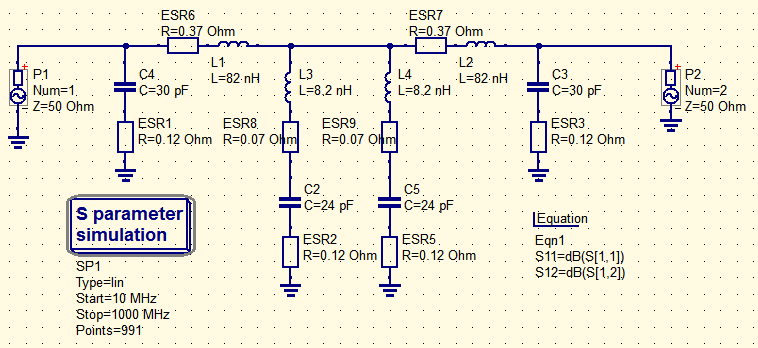
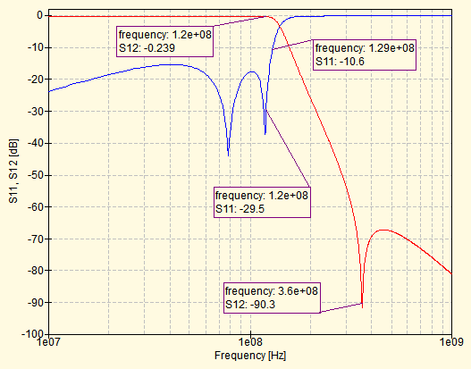
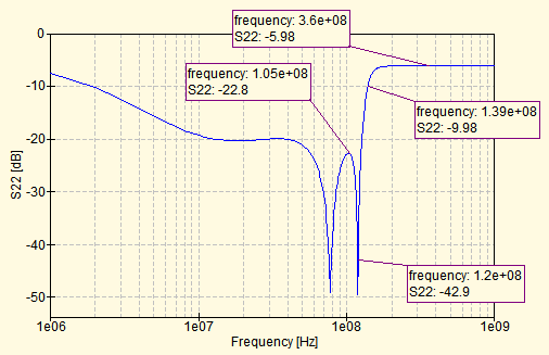
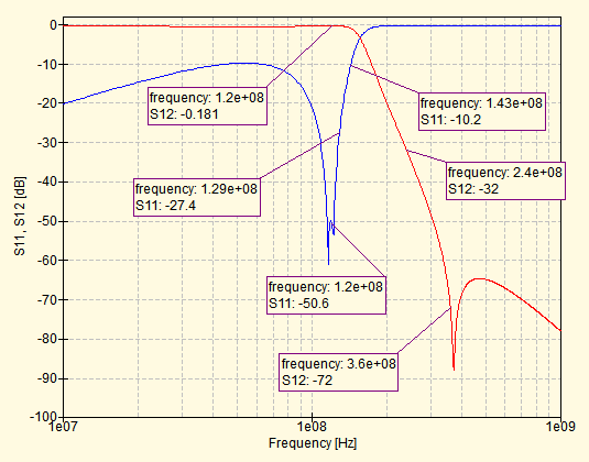
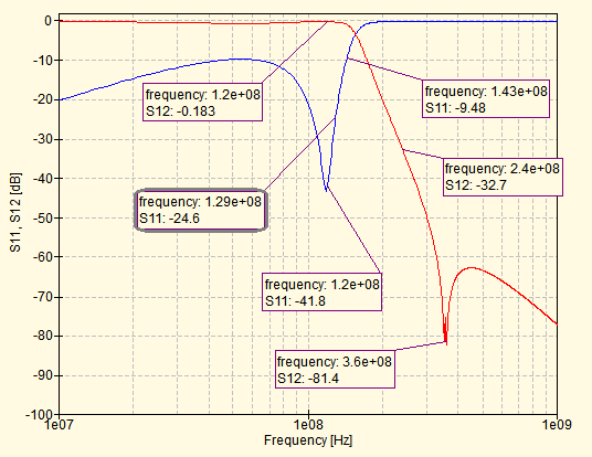
The filter can be further improved through some tweaking of the values by hand. The simulated S12 shows two notches, but these can be made to coincide by reducing the inductance values to 62 nH and 6.8 nH and increasing C2 and C5 to 27 pF. Simulations show a marked improvement in S12 at 120 MHz, as well as a wider bandwidth, but also that the third harmonic notch has shifted slightly. The notch can’t be shifted back using standard component values, and although introducing an asymmetry in the central component values does widen this notch, this is undesirable with a CPW layout.
Activity Log
2014-06-22: Revision 1.0
First batch of boards have arrived, as well as parts. I ordered the wrong size of resistor for the attenuator, but that’s no big deal. Unfortunately, it seems the footprint I created for the LT1711 places the feet too close together, too much to compensate for.
- Reflowed one board with an LT1711 in place, but the feet overlap other traces. Measured a 50 mV 120 MHz sine wave on the output pin of the oscillator, however, so it’s working. Not sure if the low voltage is due to incorrectly driving the enable pin, or due to it exceeding the oscilloscope’s bandwidth (not indicated).
- Reflowed a second board with a jumper in the place of the comparator, and no output attenuator. Measured 550 mV on the output SMA connector.
Issues
- Need a faster scope, or at least a prescaler. Should probably prototype the board with a lower frequency crystal if none is available, but that would require a different filter.
- The data sheet for the 120 MHz crystal does not indicate how to drive the enable pin. Similar crystals say to leave it open to enable the device, so the rev. 1 board does so.
- Need a better 3.3 V power supply, as the current one hacked together from another prototype appears to be unstable.
Further Changes
- The second output capacitor at the SMA connector, C5, is redundant and, if paired with a board with an input capacitor directly at the connector, will allow the connecting coax to float.
- The bridges under the CPW will change the impedance, so remove except where really necessary.
- A test pad should be connected to the oscillator’s enable pin just in case, as the pin cannot be reached directly once soldered.
2014-07-12: Revision 1.1
New batch of boards, this time with the correct footprints. I’ve also now built a small 3.3 v supply, so don’t have any more problems with that instability. The board works, producing a 120 MHz signal, but because the scope I have here is limited to 0.02 μs / div and has a 100 MHz probe, I can’t really get a reliable measurement from it.